6" Fab Sale
Wafer Foundry Facility and Building For Sale
WAFER FOUNDRY HIGHLIGHTS
Pure Play 150 MM Semiconductor Wafer Foundry
Description: 150MM Semiconductor Wafer Foundry / R&D Facility
Fab Construction Year: 2009
- WAFER FOUNDRY.CO owns and operates a Bipolar, BiCMOS, MEMS, etc. 150mm and 100mm Semiconductor Wafer Foundry.
- The wafer foundry has capacity to support a potential run rate of 10,000 wafers per year, with potential revenue of $10M/year within two years
- Currently, the wafer foundry is the only 150mm Pure-play Bipolar, BiCMOS, MEMS, etc. wafer foundry in Silicon Valley and can be repurposed for GaN and SiC.
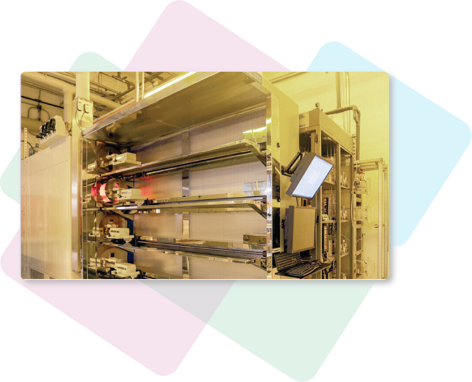
- The installed wafer fabrication equipment and infrastructure is compatible with many legacy technologies for aviation, space, communications, automotive, biomedical, MEMS, defense, analog, digital and RF ICs and many types of discrete semiconductors
INVESTMENT HIGHLIGHTS
Pure Play 150 MM Semiconductor Wafer Foundry
Location: 2108 Bering Drive, Bldg. B, San Jose, CA 95131
Building: 5,998 SF Industrial / R&D Condominium
Lot Size: 13,225 SF | 0.30 AC
Year Built: 1977
- 2108 Bering Drive, Bldg. B, San Jose is an opportunity to purchase a 5,998 SF Industrial / R&D condo fully built out as a 150mm semiconductor wafer foundry. The property is available for sale or for lease with the equipment/ facility being offered for sale or lease as well.
- The property has 1 roll-up door with a building clear height of 16ft. This is a very rare Owner User opportunity to purchase or lease a 150mm semiconductor wafer foundry in a market with very high barriers to entry. The property is strategically positioned on Bering Drive, situated between Charcot Avenue and E Brokaw Road with immediate access to Hwy 101, HWY 87, and HWY 880 and within 1 mile from San Jose airport.
Facility and Equipment List
Manufacturing Equipment
- Deposition & Growth
- Diffusion Furnace Banks (Optional):
- 1x2 200mm / MRL / High-Temperature Silicon Carbide Tubes
- 2x4 200mm THERMCO
- LPCVD (4): Protemp - Custom Build
- Vacuum Sputtering Deposition: MRC -903 - Cryo Pumped
- Diffusion Furnace Banks (Optional):
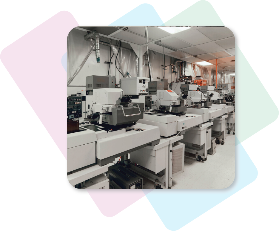
- Lithography
- Stepper (1): Canon 2500i2
- Etch & Cleaning
- Spin Coater: SVG 8100
- Plasma Etchers (4): Lam Research 409, 509
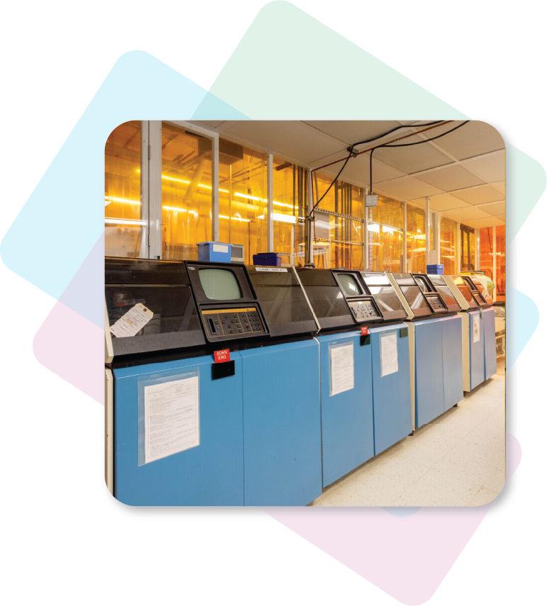
- Implantation
- Ion Implanter (2): Varian 300XP
Cleanroom Facilities
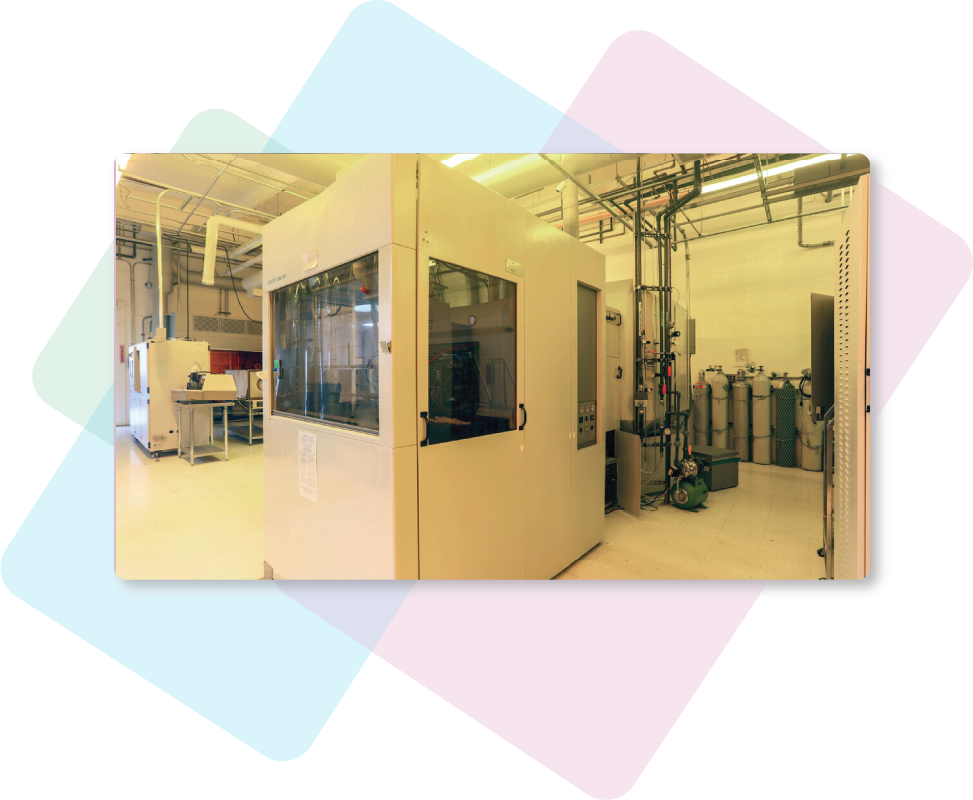
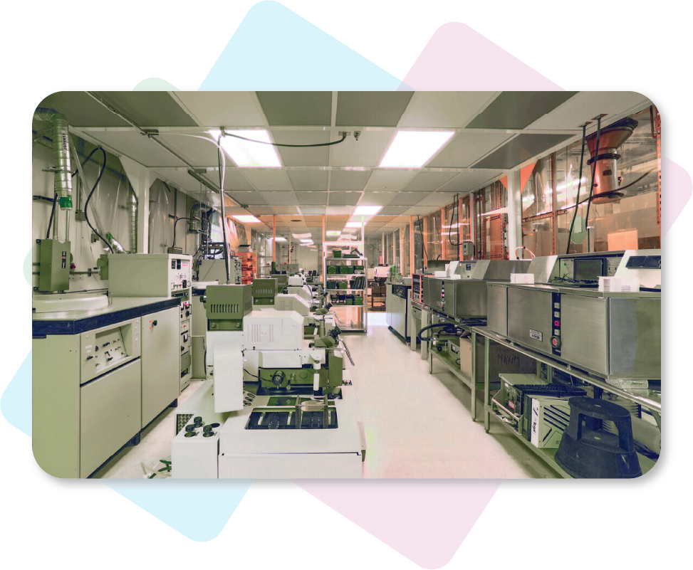
- Configuration: Bay and chase design for optimal workflow
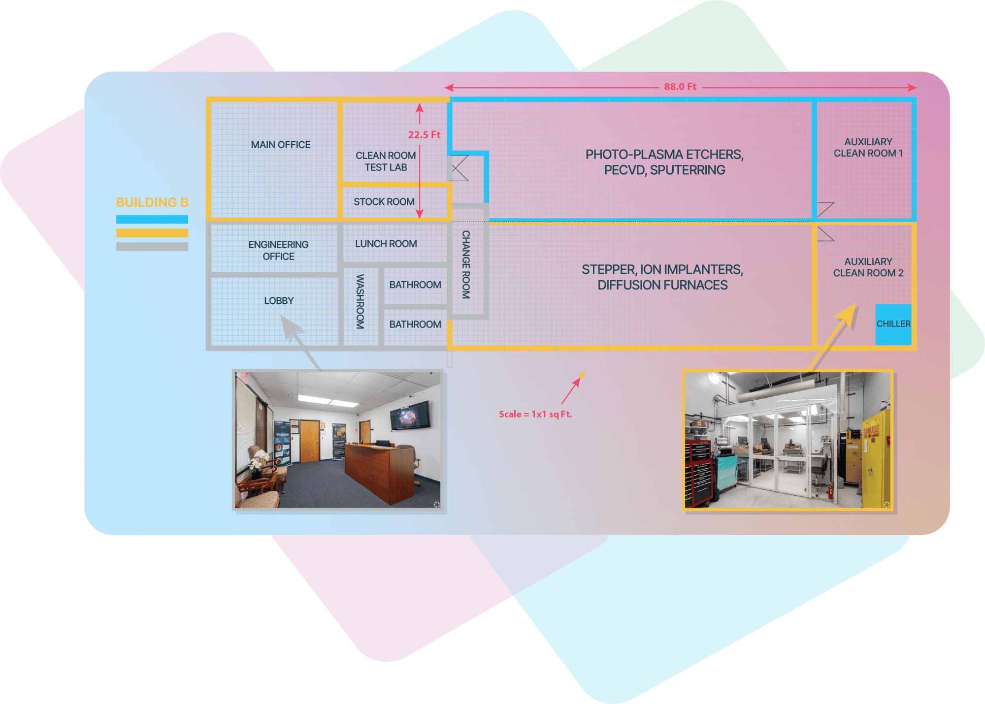
- Class 100 Cleanroom: 1,100 sq. ft.
- Class 1000 Cleanroom: 3,100 sq. ft.
- 2 Additional Clean Rooms: ~350 sq. ft. (for specialized processes)
Support Infrastructure
- Power: 208V, 3-phase, 600 Amp service
- Water:
- City water supply
- AWN wastewater treatment system
- 100 gal/hr deionized (DI) water
- Gas & Exhaust:
- N2 generator for bulk and generated gases
- Exhaust system for process byproducts
- No Backup Generators
- Climate Control:
- Chillers for cooling
- 16 ft. ceiling heights
- Production Capacity: 1,000 wafers per month (6-inch equivalent)
- Production Since: 2010
- Product Focus: Bipolar and BICMOS devices (>1um)
Cleanroom Equipment
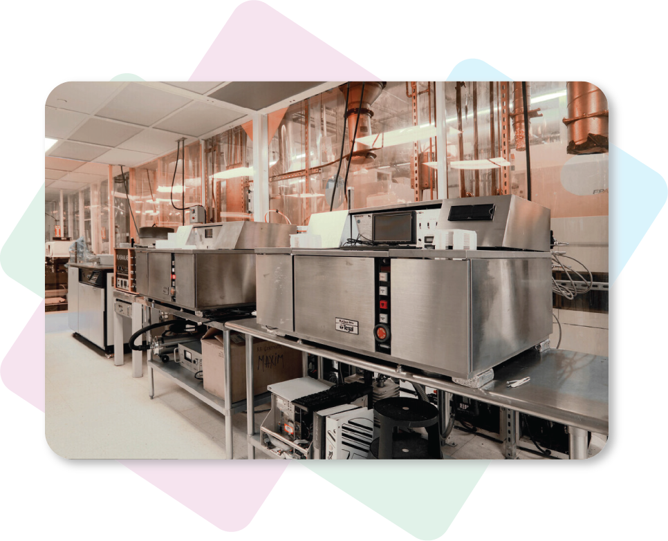
- Sputter Deposition Systems (5)
- E-Beam Evaporator
- High-Temperature Furnaces (Silicon carbide tubes)
- LPCVD Capabilities: Si3N4, a-Si, LTO, POCl3
- PECVD: AMAT 3000
- Plasma Oxygen Asher
- Solvent Bench
- Acid/Base Benches
- Photo-Resist Spinners
- Rinse/Dryer Tools
- IPA Dryer
- Mega Sonic Cleaning
- Ultrasonic Cleaning
- Ellipsometers
- Programmable Ovens
- 5X Stepper (0.45um)
- Plasma Etchers: Lam 409, 509 (4+)
- Plasma Etchers: Lam 901, 903
- EPI Reactors: AMAT 7600 (not installed – warehouse), First Nano (in-process installation)
- Ion Implanters (2pc): 300XP
- Laser Trimmers (2pc): LTX 80 Win 44
- Dicing Saws (4pc): MA1006, MA1100
- Dicing Saw: K&S
- SEM: Hitachi
- HP 4145B Semiconductor Parameter Analyzer
- Tektronix Curve Tracers
- Fluke 8840A, Keithley Multimeters
- Wire Bonders, Die Attach
Process Capabilities
- Photolithography
- Wet Chemical Processes
- Dry Silicon Etching
- Thermal Oxidation
- Ion Implantation & Diffusion
- Thermal Annealing
- Evaporation
- Sputtering
- Plasma Ashing
- Mega Sonic Cleaning
- Ultrasonic Cleaning
- Liftoff
- Film Thickness Measurement
- SEM
Centralized Utiliites
- Deionized (DI) Water
- Nitrogen Generation
- Comprehensive Piped Waste Management System (AWN)
- Compressed Air (multiple generators)
- Vacuum System
- Chilled Water (multiple sources)
- Fire and Security Monitoring System
- Dedicated Power Supply (480V, 208V, 3-phase)
- High-Speed Internet
Floor Plan
Disclaimer
This is provided for informational purposes only to prospective purchasers. Neither the owner nor Moov makes any express or implied representation, warranty, covenant, or any other agreement of any kind whatsoever related to the facility. Any negotiations or discussions between the owner and prospective purchasers will be conducted through Moov.